


How to choose a bias tee?
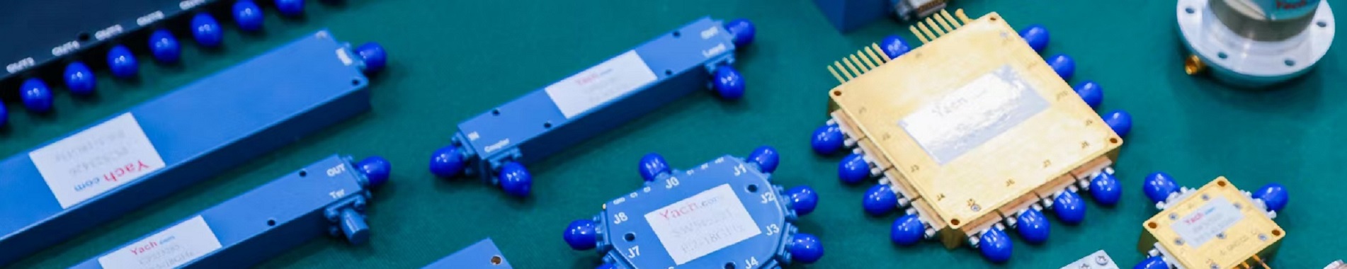
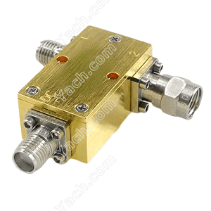
Bias tee (DC bias-t) is a three port network device. The three ports are RF port RF, DC bias port DC and RF DC port RF & DC. Because these three ports are often arranged in the shape of T, they are called bias-t.
The DC port of bias tee consists of a feeding inductor,
which is used to add DC bias to prevent the AC signal of RF port from leaking
to the power supply system. Ideally, the DC terminal will not have any impact
on the RF terminal signal; The RF port is composed of a blocking capacitor,
which is used to input the RF signal and block the DC voltage of the bias port
at the same time; The RF & DC port is connected to the device, which can see
the DC bias voltage and RF signal at the same time. If the internal device of
bias-tees selects ultra wideband, near idealized high-frequency inductance and
capacitance without resonance point, when bias-t is used to set the DC bias
point of some electronic components, it will not interfere with other
components.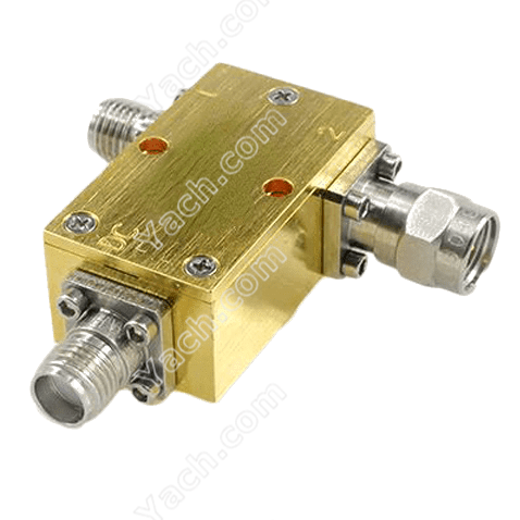
For bias tees, the more important indicators are DC terminal bias voltage and current; Isolation between RF end and DC end; RF bandwidth, group delay, insertion loss and return loss. Next, the meaning of each index will be explained separately.
DC terminal bias current
The DC terminal bias current is the current input from the DC terminal and passing through the inductance, which is mainly limited by the maximum current that the DC port inductance can withstand. The greater the value of DC terminal bias current, the better the representative index. When the actual current exceeds the upper limit of the bias current, the inductance of the DC port is in the current saturation state. The performance of bias will be affected in this state, and the device may be damaged due to excessive current, resulting in the failure of bias to work normally.
Isolation between RF end and DC end
Isolation refers to the ability of the inductance to prevent the RF signal of the RF port from flowing to the DC port, which is usually expressed in dB. Theoretically, the greater the isolation, the better. If the isolation index of a bias is poor, the RF signal will leak into the power supply system and affect the system performance. Figure 1-2 shows the schematic diagram of isolation between RF end and DC end. In the figure, the input signal power of RF port is 40dbm. When the isolation is 10dB, the signal power received at DC end is 30dBm, equivalent to 1W, which may cause irreparable damage to the power supply system; When the isolation is 40dbm, the signal power received at the DC end is 0dbm, equivalent to 1MW, which will not cause interference or damage to the power supply system.
Insertion loss
The insertion loss of bias refers to the signal attenuation between RF input and RF & DC, and the unit is usually expressed in dB.
Where UT is the transmitting signal voltage and ur is the receiving signal voltage. The insertion loss can be evaluated with the S21 parameter of the network analyzer. The insertion loss reflects the transmission path of the system. The smaller the value of the insertion loss, the better the representative index. Figure 1-3 shows the S21 parameter test diagram of a typical bias. It can be seen from the figure that the insertion loss of bias tees is about 0.5dB at the frequency point of 5GHz; At the frequency point of 30ghz, the insertion loss of bias is about 1.3db. 0.5dB < 1.3db indicates that the insertion loss index of 5GHz is better. The smaller the absolute value of insertion loss is, the better the index is.
RF bandwidth
RF bandwidth is the frequency range between the upper 3dB cut-off point and the lower 3dB cut-off point, that is, the passband of bias. The 3dB frequency cut-off point is the point where the average power in the passband is attenuated by 3dB. The wider the bandwidth of RF, the better. If the signal frequency range exceeds the passband of bias, the signal outside the passband of bias will be greatly attenuated.
Figure 1-4 shows the schematic diagram of RF bandwidth. It can be seen from the figure that the upper 3dB cut-off point is about 15GHz and the lower 3dB cut-off point is about 7GHz, so the passband is from 7GHz to 15GHz. If a 5GHz signal is input into the equipment, the signal will be attenuated by 15dB. If a 10GHz signal is input into the equipment, the signal will be attenuated by 1dB, that is, the signal attenuation in the RF passband is reduced, and the signal outside the passband is greatly attenuated. It can be concluded that the larger the RF bandwidth, the larger the signal frequency range allowed to pass normally.
Return loss
Return loss, also known as reflection loss, is the ratio of reflected wave power and incident wave power at the transmission line port. It is expressed in logarithmic form. The unit is dB, which is generally negative. It can be evaluated by S11 and S22 parameters of the network analyzer. Return loss is an index used to measure the link impedance mismatch. Unqualified return loss means that the data transmission system is in the state of impedance mismatch. The lower the value of return loss, the smaller the return loss, and the less the signal reflection and signal distortion. Generally, the return loss is kept between - 20dB and - 40dB.
Among them, RL is the abbreviation of return loss, P reflection refers to the power of the reflected signal, and P incidence refers to the power of the incident signal.
Group delay
Group delay refers to the change rate of the phase (phase shift) of the system at a certain frequency to the frequency. When the broadband signal passes through the medium transmission path or linear components in the equipment, the phase velocity of each spectrum component is different, and the response of components to each spectrum component is also different, which will cause the disorder of phase relationship of the signal arriving at the receiving end due to the different phase shift or delay of each frequency component, that is, phase distortion. The ideal group delay curve should be a straight line without fluctuation. The smaller the vibration amplitude of group delay, would be better.
For bias tees, the smaller the change of group delay, the smaller the influence of signal. If the bias group delay of an access system changes greatly, it will lead to the phase distortion of the signal, and an obvious phase shift can be observed on the oscilloscope.
Bias tees can be applied to all fields from chips to test
and measurement equipment and systems. Biast is mainly used to supply power to
transistors or amplifier circuits and drive electro-optic modulators and
lasers.
Broadband amplifier
Bias tees can be used for the feed of broadband amplifier, which is a very mature application. The amplifier that needs power supply at the output requires bias-t to be added to provide stable working conditions for the amplifier.
When the amplifier needs to add bias-t to feed, focus on some indicators of bias tees: bias-t passband, maximum input power at RF end, S21 parameter, S22 parameter, S11 parameter, rise and fall time, jitter, etc.
When purchasing bias tees, the first step should be to determine the frequency range of the amplifier and the frequency range of bias tees. Figure 1-8 shows the schematic diagram of the frequency band connected between the amplifier and bias-t. In the figure, the frequency range of the amplifier is from 40KHz to 40GHz, and the frequency range of bias is from 50KHz to 18GHz. After the two are connected, the passband is the overlapping part of the frequency range of the two. Outside the band of bias-t, such as 18GHz to 40GHz, the signal will have great loss and cannot achieve the expected effect of the amplifier. Therefore, when selecting bias tee, make sure that the passband range of bias is greater than or equal to the frequency range of broadband amplifier.
- ÉÏŌŧÆŠĢšWhat's the bias tees? [2022-05-03]
- ÏÂŌŧÆŠĢšWorking principle and application of coupler [2021-12-06]