


What is the bias tee circuit
2022-05-04 17:58:52 ĩãŧũĢš
 The bias tee seems like a simple thing, but if you need more than a decade of bandwidth, you know that designing one is not trivial. Here's a great video on basic bias tees' design, showing how inductors are cascaded to perform over frequency with the usual caveat that lumped elements present all kinds of non-ideal issues at microwave frequencies. Designing a bias-t is like designing a speaker cross-over network for audio.
Perhaps the hardest thing about designing a bias-t is obtaining accurate modeling data on the inductors you will need. We'll try our hand at this one of these days.
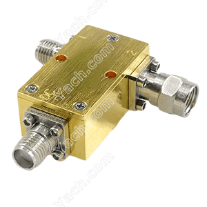
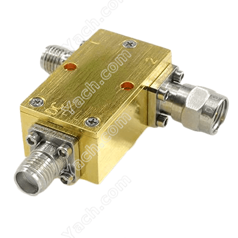
The bias tees are used to supply DC currents or voltages to RF devices, such as the FETs that are used in amplifiers. Bias-Ts are everywhere, from your cell phone's power amp to the front panel of your network analyzer. The bias tees are a classic example of a diplexer In the figure below, an RF signal incident to the upper right port (labeled RF & DC)is delivered only to the upper left port (RF only). A DC signal (or very low frequency, or video, signal) can be passed from the upper right port to the lower right port (DC only). Properties that are important to a bias tee are RF bandwidth, insertion loss and mismatch at the two RF ports, the maximum DC current, and video bandwidth of the DC port.
A simple bias tee
Another consideration is DC current carrying capability. As a general rule of thumb, try to restrict the temperature rise of inductors to 100C or less, this will set the practical limit on what current you can source though a bias tee design. DC resistance of the inductor can be used to calculate the voltage drop and power dissipated in a bias tee. An honest accounting of solid-state power amplifier would take this heat into account.
"Pulsed" bias tees have reduced video isolation, allowing a current pulse reach the amplifier with minimum distortion. All MMIC power amplifiers that are RF tested on-wafer should be tested in pulsed DC mode so they don't overheat. The usual modification is to reduce the bypass capacitor on the DC only terminal to something that only blocks the RF band and nothing else. 100 pF might be a good value for a pulsed bias tee at X-band and still pass microsecond drain pulses with good rise/fall times. Try out your SPICE skills on this problem before you make hardware.
The schematic above cannot be applied to wideband bias tees, additional tricks are involved in order to use non-ideal inductors. Get in touch with us if you want to share information on wideband bias-t techniques, or send us some questions and we can work on it together.
- ÉÏŌŧÆŠĢšHow to use a bias tee? [2022-05-04]
- ÏÂŌŧÆŠĢšHow does a bias tee work? [2022-05-04]